AXI and Memory Interface
Field
Reconfigurable Computing
Institution
RIT
Year
2023
Project Type
Individual Project
Course
Reconfigurable Computing
Keywords
FPGA, AXI stream interface, BRAM, Testbench, DDR2 memory integration, UART, AXILite interface, MIG, FIFO, State machines, Vivado
This project delves into the development of an FPGA-based system designed for advanced data storage and retrieval. Structured in three key phases, it begins with establishing an SXI stream interface with BRAM, progresses to crafting a testbench capable of processing data and commands from external files, and culminates in integrating the system with DDR2 memory, enhancing its capability beyond BRAM. The architecture utilizes UART, FPGA’s block RAM, DDR2 memory, and the AXILite interface, ensuring smooth communication between BRAM/DDR2 and the MIG. This allows for efficient data manipulation and retrieval, laying a robust foundation for handling complex datasets such as image files. The project showcases the potential for scalable and flexible data management systems powered by FPGA technology.
Design methodology
This section delves into the foundational aspects of interfacing and data handling within an FPGA-based system, structured into three distinct parts to build comprehensive skills in FPGA programming and system design. Each stage of this exercise progressively builds on the last, from basic data interfacing to complex system integration, highlighting the intricacies and potential of FPGA-based data management systems.
-
AXI Stream to Lite Interface with BRAM:
-
Establishes basic understanding of data flow between UART and BRAM.
-
Data is read and stored in 4-byte segments, facilitating both input to and retrieval from BRAM.
-
-
DDR2 Memory Integration:
-
Provides insights into integrating DDR2 memory for expanded system capabilities, despite challenges in simulation-to-hardware functionality translation.
-
Demonstrates the system's potential for scalability and flexibility in handling more complex memory systems.
-

RTL diagram for interface process


FIFO to BRAM state diagram
BRAM to FIFO state diagram

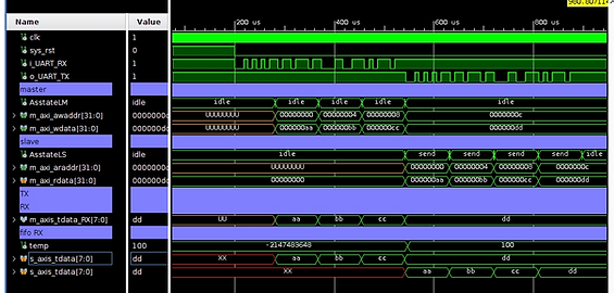
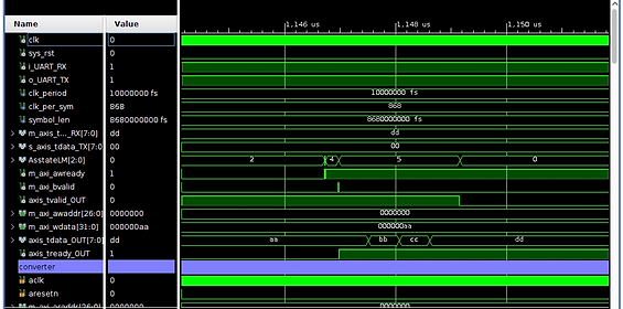
waveform output with advanced testbench

waveform output with advanced testbench

waveform output with advanced testbench
Result and analysis
This section delves into the evaluation and testing phase of the FPGA-based data storage and retrieval system, highlighting the intricate dynamics between hardware components and simulation processes. Key insights were gained through the use of both simple and advanced testbenches, underscoring the system's functionality and potential areas for refinement. This phase underscores the project's commitment to rigorous testing and continuous improvement, setting a foundation for future enhancements and integration with more complex memory systems.
-
Demonstrated data flow from UART to BRAM and back, utilizing state machine logic to manage data handling and output.
-
Advanced testbench facilitated automated testing, allowing for dynamic scenario testing based on external command files.
-
The testbench's output logging provided valuable feedback on system performance, with outputs recorded in binary format.
-
Simulation results showcased the intended system functionality with BRAM, and attempts were made to extend this to DDR2 memory, reflecting the system's adaptability and scalability despite challenges in fully implementing the DDR2 interface.
This project delved into the nuances of various memory systems compatible with Vivado and our specific hardware setup. Structured in a sequential manner. The journey through this exercise shed light on practical FPGA applications, encompassing fundamental data management, storage techniques, and the automation of testing procedures. It imparted crucial insights into the execution of hardware testing and integration, with a particular focus on overcoming the challenges associated with integrating sophisticated memory systems like DDR2. This endeavor underscored the critical importance of understanding both hardware and software interfaces, especially when dealing with complex memory configurations.